- 您现在的位置:买卖IC网 > Sheet目录1193 > AD8348-EVALZ (Analog Devices Inc)BOARD EVAL FOR AD8348
�� ��
��
��AD8348�
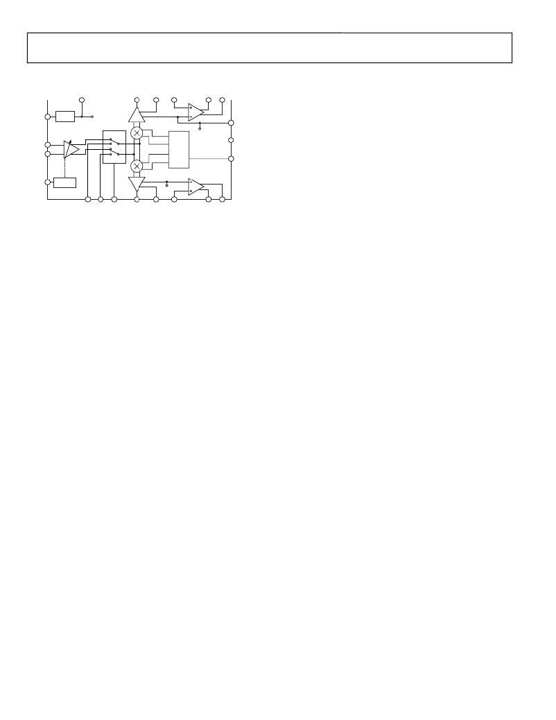
�THEORY� OF� OPERATION�
�ENBL� 15�
�BIAS�
�CELL�
�VREF�
�14�
�VREF�
�IMXO�
�8�
�IOFS�
�13�
�IAIN�
�6�
�DIVIDE�
�IOPP�
�4�
�VCMO�
�IOPN�
�3�
�5�
�1�
�VCMO�
�LOIP�
�PHASE� SPLITTER�
�Quadrature� generation� is� achieved� using� a� divide-by-2� frequency�
�divider.� Unlike� a� polyphase� filter� that� achieves� quadrature� over�
�a� limited� frequency� range,� the� divide-by-2� approach� maintains�
�IFIP� 11�
�BY� 2�
�quadrature� over� a� broad� frequency� range� and� does� not� attenuate�
�IFIN� 10�
�PHASE�
�SPLITTER�
�28�
�LOIN�
�the� LO.� The� user,� however,� must� provide� an� external� signal� XLO�
�AD8348�
�that� is� twice� the� frequency� of� the� desired� LO� frequency.� XLO� drives�
�VGIN� 17�
�GAIN�
�CONTROL�
�VCMO�
�the� clock� inputs� of� two� flip-flops� that� divide� down� the� frequency�
�by� a� factor� of� 2.� The� outputs� of� the� two� flip-flops� are� one-half�
�18� 19� 24�
�MXIP� MXIN� ENVG�
�21�
�QXMO�
�16�
�QOFS�
�23�
�QAIN�
�25� 26�
�QOPP� QOPN�
�period� of� XLO� out� of� phase.� Equivalently,� the� outputs� are� one-�
�Figure� 48.� Functional� Block� Diagram�
�VGA�
�The� VGA� is� implemented� using� the� patented� X-AMP� architecture.�
�The� single-ended� IF� signal� is� attenuated� in� eight� discrete� 6� dB�
�steps� by� a� passive� R-2R� ladder.� Each� discrete� attenuated� version�
�of� the� IF� signal� is� applied� to� the� input� of� a� transconductance�
�stage.� The� current� outputs� of� all� transconductance� stages� are�
�summed� together� and� drive� a� resistive� load� at� the� output� of� the�
�VGA.� Gain� control� is� achieved� by� smoothly� turning� on� and�
�off� the� relevant� transconductance� stages� with� a� temperature-�
�compensated� interpolation� circuit.� This� scheme� allows� the� gain�
�to� continuously� vary� over� a� 44� dB� range� with� linear-in-decibel�
�gain� control.� This� configuration� also� keeps� the� relative� dynamic�
�range� constant� (for� example,� IIP3� ?� NF� in� dB)� over� the� gain�
�setting;� however,� the� absolute� intermodulation� intercepts� and�
�noise� figure� vary� directly� with� gain.� The� analog� voltage� VGIN�
�sets� the� gain.� VGIN� =� 0.2� V� is� the� maximum� gain� setting,� and�
�VGIN� =� 1.2� V� is� the� minimum� voltage� gain� setting.�
�DOWNCONVERSION� MIXERS�
�The� output� of� the� VGA� drives� two� (I� and� Q)� double-balanced�
�Gilbert� cell� downconversion� mixers.� Alternatively,� driving� the�
�ENVG� pin� low� can� disable� the� VGA,� and� the� mixers� can� be�
�externally� driven� directly� via� the� MXIP� and� MXIN� ports.� At�
�the� input� of� the� mixer,� a� degenerated� differential� pair� performs�
�linear� voltage-to-current� conversions.� The� differential� output�
�current� feeds� into� the� mixer� core� where� it� is� downconverted� by�
�the� mixing� action� of� the� Gilbert� cell.� The� phase� splitter� provides�
�quadrature� LO� signals� that� drive� the� LO� ports� of� the� in-phase�
�and� quadrature� mixers.�
�Buffers� at� the� output� of� each� mixer� drive� the� IMXO� and� QMXO�
�pins.� These� linear,� low� output� impedance� buffers� drive� 40� Ω,�
�temperature-stable,� passive� resistors� in� series� with� each� output�
�pin� (IMXO� and� QMXO).� This� 40� Ω� should� be� considered� when�
�calculating� the� reverse� termination� if� an� external� filter� is� inserted�
�between� IMXO� (QMXO)� and� IAIN� (QAIN).� The� VCMO� pin� sets�
�the� dc� output� level� of� the� buffer.� This� can� be� set� externally� or�
�connected� to� the� on-chip� 1.0� V� reference,� VREF.�
�quarter� period� (90°)� of� the� desired� LO� frequency� out� of� phase.�
�Because� the� transitions� on� XLO� define� the� phase� difference� at�
�the� outputs,� deviation� from� 50%� duty� cycle� translates� directly� to�
�quadrature� phase� errors.�
�If� the� user� generates� XLO� from� a� 1� frequency� (f� REF� )� and� a�
�frequency-doubling� circuit� (XLO� =� 2� � f� REF� ),� fundamentally�
�there� is� a� 180°� phase� uncertainty� between� f� REF� and� the� AD8348�
�internal� quadrature� LO.� The� phase� relationship� between� I� and� Q�
�LO,� however,� is� always� 90°.�
�I/Q� BASEBAND� AMPLIFIERS�
�Two� (I� and� Q)� fixed� gain� (20� dB),� single-ended-to-differential�
�amplifiers� are� provided� to� amplify� the� demodulated� signal�
�after� off-chip� filtering.� The� amplifiers� use� voltage� feedback� to�
�linearize� the� gain� over� the� demodulation� bandwidth.� These�
�amplifiers� can� be� used� to� maximize� the� dynamic� range� at� the�
�input� of� an� ADC� following� the� AD8348.�
�The� input� to� the� baseband� amplifiers,� IAIN� (QAIN),� feeds� into�
�the� base� of� a� bipolar� transistor� with� an� input� impedance� of�
�roughly� 50� kΩ.� The� baseband� amplifiers� sense� the� single-ended�
�difference� between� IAIN� (QAIN)� and� VCMO.� IAIN� (QAIN)�
�can� be� dc� biased� by� terminating� it� with� a� shunt� resistor� to�
�VCMO,� such� as� when� an� external� filter� is� inserted� between�
�IMXO� (QMXO)� and� IAIN� (QAIN).� Alternatively,� any� dc�
�connection� to� IMXO� (QXMO)� can� provide� appropriate� bias� via�
�the� offset-nulling� loop.�
�ENABLE�
�A� master� biasing� cell� that� can� be� disabled� using� the� ENBL� pin�
�controls� the� biasing� for� the� chip.� If� the� ENBL� pin� is� held� low,�
�the� entire� chip� powers� down� to� a� low� power� sleep� mode,�
�typically� consuming� 75� μA� at� 5� V.�
�BASEBAND� OFFSET� CANCELLATION�
�A� low� output� current� integrator� senses� the� output� voltage� offset�
�at� IOPP� and� IOPN� (QOPP� and� QOPN)� and� injects� a� nulling�
�current� into� the� signal� path.� The� integration� time� constant� of� the�
�offset-nulling� loop� is� set� by� Capacitor� COFS� from� IOFS� (QOFS)� to�
�Rev.� A� |� Page� 18� of� 28�
�发布紧急采购,3分钟左右您将得到回复。
相关PDF资料
AD8436-EVALZ
BOARD EVAL FOR AD8436
AD9352-5/PCBZ
EVALUATION BOARD
AD9550/PCBZ
BOARD EVALUATION FOR AD9550
AD9985A/PCBZ
KIT EVALUATION FOR AD9985A
ADA4850-2YCP-EBZ
BOARD EVAL FOR ADA4850-2YCP
ADA4899-1YCP-EBZ
BOARD EVAL FOR ADA4899-1YCP
ADA4937-1YCP-EBZ
BOARD EVAL FOR ADA4937-1YCP
ADA4938-2YCP-EBZ
BOARD EVAL FOR ADA4938-2YCP
相关代理商/技术参数
AD8348XRU
制造商:Analog Devices 功能描述:QUADRATURE MODULATOR X-GRADE - Rail/Tube
AD8348XXX
制造商:AD 制造商全称:Analog Devices 功能描述:50-1000 MHz Quadrature Demodulator
AD8349
制造商:AD 制造商全称:Analog Devices 功能描述:400 MHz to 6 GHz Broadband Quadrature Modulator
AD8349ARE
制造商:Analog Devices 功能描述:Quadrature Mod 160MHz 16-Pin TSSOP EP Tube 制造商:Rochester Electronics LLC 功能描述:DIRECT QUADRATURE MODULATOR - Bulk 制造商:Analog Devices 功能描述:IC MODULATOR QUADRATURE
AD8349ARE-REEL7
功能描述:IC QUADRATURE MOD 700MHZ 16TSSOP RoHS:否 类别:RF/IF 和 RFID >> RF 调制器 系列:- 产品培训模块:Lead (SnPb) Finish for COTS
Obsolescence Mitigation Program 标准包装:2,500 系列:- 功能:调制器 LO 频率:700MHz ~ 2.3GHz RF 频率:700MHz ~ 2.3GHz P1dB:1dBm 底噪:-148dBm/Hz 输出功率:-1dBm 电流 - 电源:46mA 电源电压:2.7 V ~ 3.6 V 测试频率:1.75GHz 封装/外壳:28-WFQFN 裸露焊盘 包装:带卷 (TR)
AD8349AREZ
功能描述:IC QUADRATURE MOD 700MHZ 16TSSOP RoHS:是 类别:RF/IF 和 RFID >> RF 调制器 系列:- 产品培训模块:Lead (SnPb) Finish for COTS
Obsolescence Mitigation Program 标准包装:2,500 系列:- 功能:调制器 LO 频率:700MHz ~ 2.3GHz RF 频率:700MHz ~ 2.3GHz P1dB:1dBm 底噪:-148dBm/Hz 输出功率:-1dBm 电流 - 电源:46mA 电源电压:2.7 V ~ 3.6 V 测试频率:1.75GHz 封装/外壳:28-WFQFN 裸露焊盘 包装:带卷 (TR)
AD8349AREZ-RL7
功能描述:IC MOD QUAD 2.7GHZ 16TSSOP RoHS:是 类别:RF/IF 和 RFID >> RF 调制器 系列:- 产品培训模块:Lead (SnPb) Finish for COTS
Obsolescence Mitigation Program 标准包装:2,500 系列:- 功能:调制器 LO 频率:700MHz ~ 2.3GHz RF 频率:700MHz ~ 2.3GHz P1dB:1dBm 底噪:-148dBm/Hz 输出功率:-1dBm 电流 - 电源:46mA 电源电压:2.7 V ~ 3.6 V 测试频率:1.75GHz 封装/外壳:28-WFQFN 裸露焊盘 包装:带卷 (TR)
AD8349EVAL
制造商:Analog Devices 功能描述:IC ((NS))